The new era of semiconductors will enable transformational products for artificial intelligence (AI), 5G, automotive, networking, cloud and edge compute applications. Ubiquitous connectivity, low latency and faster data rates will enable billions of more smart devices. These devices will rely on advanced, low power FinFET designs and state-of-the-art 3D-IC packaging technologies to deliver the required power, performance, area and reliability metrics.
Multiphysics analysis is critical for enabling these cutting-edge electronics systems to work reliably in their lifetime. ANSYS empowers customers with multiphysics simulations to simultaneously solve power, thermal, variability, timing, electromagnetics and reliability challenges across the spectrum of chip, package and system to promote first-time silicon and system success. ANSYS simulation and modeling tools offer you early power budgeting analysis for high-impact design decisions and foundry-certified accuracy needed for IC signoff.
System-aware IC power efficiency, power integrity and reliability
At the core of every electronics system is a chip that has to meet multiple conflicting requirements, such as high performance, increased functionality, power efficiency, reliability and low cost. Ensuring the chip meets power efficiency, power integrity and reliability requirements as both a stand-alone component and within the electronics system calls for a system-aware chip design methodology. ANSYS uniquely offers a suite of multiscale, multiphysics solutions to support a chip-package-system (CPS) design flow.
Foundry certified accuracy
With the cost of designing and implementing a system-on-chip (SoC) ranging from $50 million to $200 million, first-time working silicon is a must. IC designers require the most accurate simulation solution and consider foundry certification as the ultimate proof of accuracy. ANSYS semiconductor solutions have been certified by all leading foundries since 2006.
Production-proven solutions
Our software has enabled thousands of successful tape-outs across multiple technology nodes. Our solutions are used by more than 90 percent of the global semiconductor companies, including all of the top 20.
Applications
Products

RedHawk
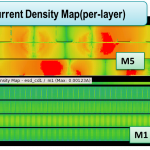
RedHawk is the standard for power integrity and reliability solutions. It accurately predicts chip power and noise using voltage drop simulation analysis for the entire power delivery
network (PDN), from chip to package to board.
Totem
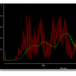
Totem is a transistor-level power noise and reliability simulation platform for analog, mixed-signal and custom digital designs.
PowerArtist
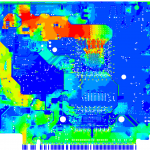
PowerArtist is a comprehensive physically-awaredesign-for-power solution for early register-transfer-level (RTL) power budgeting, efficiency analysis, reduction and regression. It can profile the power of real applications and perform seamless RTL-to-physical power integrity and thermal analysis.

PathFinder
Planning, verification and sign-off solution for IP and SoC
RedHawk-S.C.
EDA for big data and elastic compute architecture
Path FX
Path-based timing analysis for an entire SoC
Variance FX
Inductive device synthesis and modeling
RaptorX
RaptorX is a novel pre-LVS electromagnetic modeling software with limitless capacity of its engine in combination with highly accurate results and blazing fast modeling times.

